AGS-M1
Three-axis fluxgate magnetometer board
A 24-bit acquisition board for a fluxgate sensor, yours or one we supply, with checksummed framing, on-board recording and a three-axis accelerometer. It runs from its own 8 MHz clock, or from your system's on firmware we send on request. It is designed to sit inside your instrument and answer to your host.
Every value says where it comes from.
| PARAMETER | VALUE | EVIDENCE |
|---|---|---|
| PERFORMANCE | ||
| Chain noise floor | 0.035 nT/√Hz, inputs shorted at the sensor connector, converter at 503.8 S/s | MEASURED |
| Output rates | 10 / 50 / 100 / 200 S/s | MEASURED |
| Continuity | 6,200 samples recorded on board at 200 S/s, none missed | MEASURED |
| External clock | Runs from your 8 MHz master clock on J3 pin 5, and stops cleanly if it is lost, on the clock-following firmware we send on request (one board, 4 of 4 tests, July 2026) | MEASURED |
| Field record | Industrial site, September 2026 | FIELD-TESTED |
| SENSING | ||
| Sensor | Supplied on request (Bartington Mag-03MCUP250, ±250 µT per axis), or connect your own three-axis fluxgate | VENDOR |
| Acquisition | 24-bit sigma-delta, multiplexed across channels | DESIGN |
| Accelerometer | Three-axis, on board; a coarse tilt witness | DESIGN |
| DATA AND INTERFACE | ||
| Host link | RS-485 half-duplex at 100,000 baud, or 3.3 V TTL serial at 921,600 baud; one link per power-up, set by a switch | DESIGN |
| Framing | CRC-32 on every frame; host-initiated poll and response | DESIGN |
| Recording | ≈35,000 samples on board; every sample checksummed; resumable, verified readback | DESIGN |
| Clock pin | J3 pin 5 carries the board's own 8 MHz as shipped; do not drive a clock into it on the shipping firmware | DESIGN |
| PHYSICAL AND POWER | ||
| Supply | 9 V nominal | DESIGN |
| Supply range | Not yet specified | OPEN |
| Power consumption | About 0.25 A at 9 V (≈2.3 W) on one board, with the fluxgate powered from the board; peak draw not yet measured | MEASURED |
| Board | 43.18 × 95.25 mm, 4 layers | DESIGN |
| Underside part height | Not yet measured | OPEN |
| Connectors | Molex PicoBlade, 1.25 mm pitch, on the top side. J4 power, 0530470410: 1–2 DC in, 3–4 ground. J3 host link, 0530470610: 1 TTL serial TX, 2 RS-485 A, 3 RS-485 B, 4 TTL serial RX, 5 8 MHz clock (the board's own as shipped; yours with the clock-following firmware), 6 sync (no function in the shipping firmware); the serial, clock and sync pins are 3.3 V logic. J3 has no ground pin: its signal ground is J4's. J2 sensor, 0530470810: 1–3 X, Y, Z in, 4 analog return, 5 supply return, 6 +12.5 V, 7 −12.5 V, 8 self-test. | DESIGN |
| Mounting | Four non-plated Ø3.175 mm holes, each 2.667 mm in from both edges at a corner: a 37.846 × 89.916 mm rectangle, for M3 or #4 screws. Keep-outs: both faces are free of copper to Ø5.3 mm and of parts to Ø6.0 mm around each hole, and copper and parts stay at least 0.63 mm in from every edge. | DESIGN |
| Mass | Not yet measured | OPEN |
| Operating temperature | Not yet specified | OPEN |
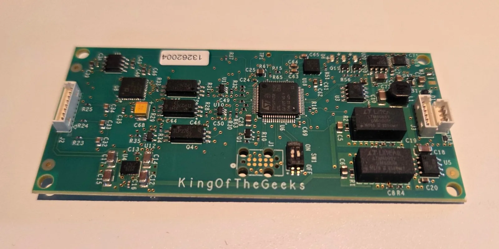
The board as built.
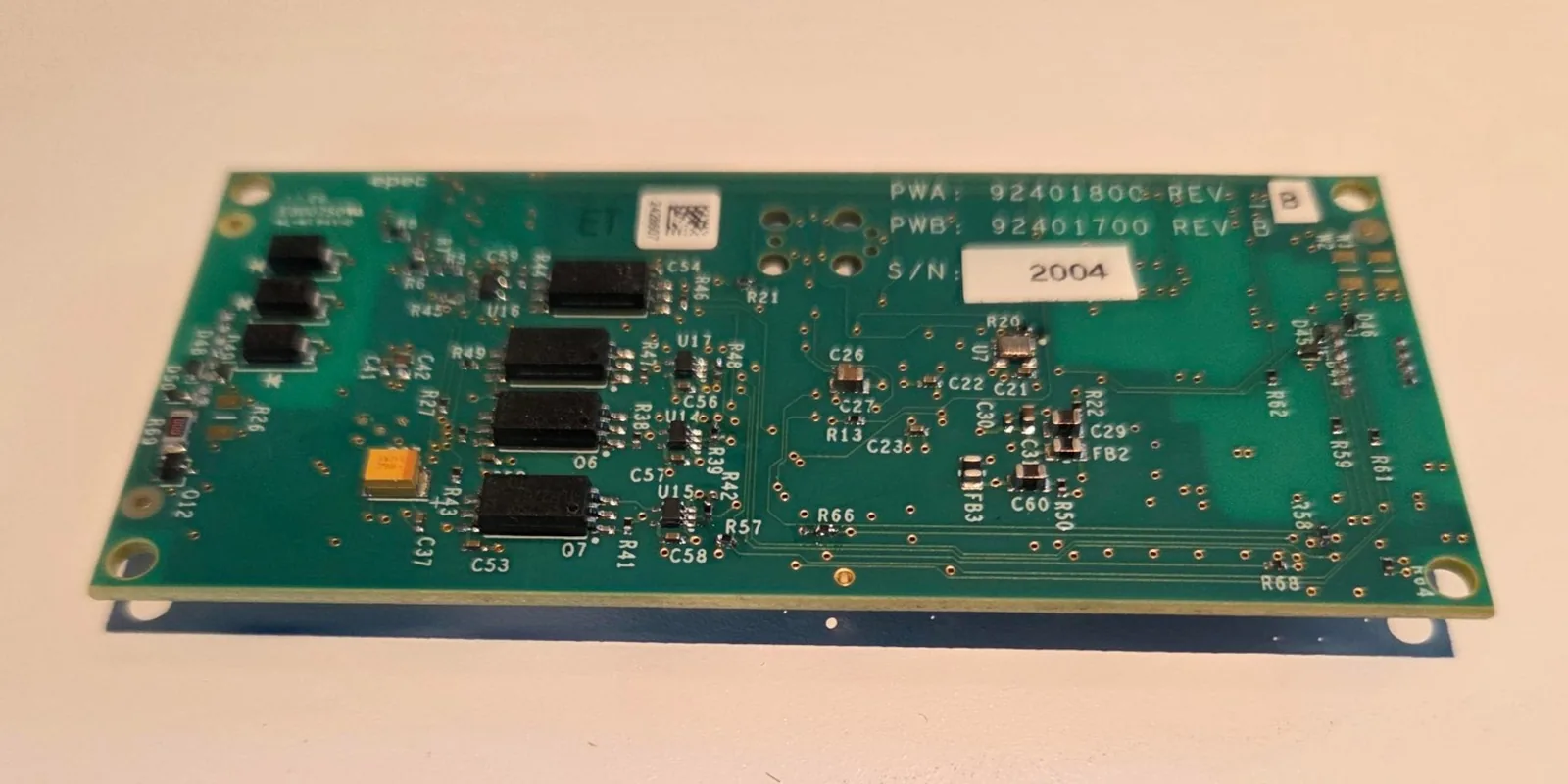
Every part is surface-mount except the three connectors, and the underside carries only low parts.
How it was measured.
- Input
- Sensor disconnected, inputs shorted at the sensor connector
- Converter rate
- 503.8 S/s, 50 S/s output
- Measured
- On our bench, on this board, July 2026; raw data kept with the report
- Method
- The reading's standard deviation divided by √(converter rate ÷ 2). Divided by √(output rate ÷ 2) instead, the same data read about 0.11 nT/√Hz
- Next
- Re-run with a shielded short, which settles the method · OPEN
It can run from your system's clock.
As shipped, the board runs on its own oscillator and drives 8 MHz out on J3 pin 5. On the clock-following firmware, which we send on request, it runs entirely from your 8 MHz master clock instead, with no hardware change: it locks, samples, and stops cleanly if the clock is lost. One board passed all four tests in July 2026. Several boards sharing one clock, so that an array samples together, is the design intent and has not been tested.
Designs that need a precise field reading.
Four kinds of design the board suits, and the property behind each.
Survey instruments
Small features in the field, resolved along a line or a grid.
Synchronized arrays
Several boards on one master clock, so readings taken together give gradients. One board has run from an external clock, on the clock-following firmware; a clock shared across an array has not been tested.
Magnetic signature testing
The field a component or assembly adds, measured before it sits beside a sensitive instrument.
Embedded in your instrument
A sensing core inside a larger product, speaking a checksummed, poll-and-response protocol.
Integrating it? Write to us first.
Email king@airandgravity.com. We will tell you where the interface document stands, and send the simulator so your host code can run before a board arrives.
IN DESIGN Rev C, the next revision of the board, is in design. Its numbers are published when it is built and measured.